Electric current in semiconductor materials. Electric current in semiconductors. Semiconductor diode. Semiconductor devices
Semiconductors are substances that have electrical conductivity intermediate position between good guides And good insulators(dielectrics).
Semiconductors are both chemical elements (germanium Ge, silicon Si, selenium Se, tellurium Te) and compounds chemical elements(PbS, CdS, etc.).
The nature of current carriers in different semiconductors is different. In some of them, the charge carriers are ions; in others, the charge carriers are electrons.
Intrinsic conductivity of semiconductors
There are two types of intrinsic conductivity of semiconductors: electronic conductivity and hole conductivity of semiconductors.
1. Electronic conductivity of semiconductors.
Electronic conductivity is carried out by the directed movement in the interatomic space of free electrons that have left the valence shell of the atom as a result of external influences.
2. Hole conductivity of semiconductors.
Hole conduction occurs with the directed movement of valence electrons to vacant positions in pair-electron bonds - holes. The valence electron of a neutral atom located in close proximity to a positive ion (hole) is attracted to the hole and jumps into it. In this case, a positive ion (hole) is formed in place of a neutral atom, and a neutral atom is formed in place of a positive ion (hole).

In an ideally pure semiconductor without any foreign impurities, each free electron corresponds to the formation of one hole, i.e. the number of electrons and holes involved in creating the current is the same.
Conductivity at which occurs same number charge carriers (electrons and holes) is called the intrinsic conductivity of semiconductors.
The intrinsic conductivity of semiconductors is usually low, since the number of free electrons is small. The slightest traces of impurities radically change the properties of semiconductors.
Electrical conductivity of semiconductors in the presence of impurities
Impurities in a semiconductor are considered to be atoms of foreign chemical elements that are not contained in the main semiconductor.
Impurity conductivity is the conductivity of semiconductors due to the introduction of impurities into their crystal lattices.
In some cases, the influence of impurities is manifested in the fact that the “hole” conduction mechanism becomes practically impossible, and the current in the semiconductor is carried out mainly by the movement of free electrons. Such semiconductors are called electronic semiconductors or n-type semiconductors(from the Latin word negativus - negative). The majority charge carriers are electrons, and the non-majority charge carriers are holes. N-type semiconductors are semiconductors with donor impurities.
1. Donor impurities.
Impurities that easily donate electrons and, therefore, increase the number of free electrons are called donor impurities. Donor impurities supply conduction electrons without creating the same number of holes.
 A typical example of a donor impurity in tetravalent germanium Ge is the pentavalent arsenic atoms As.
In other cases, the movement of free electrons becomes practically impossible, and the current is carried out only by the movement of holes. These semiconductors are called hole semiconductors or p-type semiconductors(from the Latin word positivus - positive). The main charge carriers are holes, not the main charge carriers - electrons. . P-type semiconductors are semiconductors with acceptor impurities.
Acceptor impurities are impurities in which there are not enough electrons to form normal pair-electronic bonds.
An example of an acceptor impurity in germanium Ge is trivalent gallium atoms Ga

Electricity through the contact of p-type and n-type semiconductors p-n junction- this is a contact layer of two impurity semiconductors of p-type and n-type; A p-n junction is the boundary separating regions with hole (p) conductivity and electronic (n) conductivity in the same single crystal.
Direct p-n junction
If an n-semiconductor is connected to the negative pole of the power source, and the positive pole of the power source is connected to the p-semiconductor, then under the influence electric field electrons in an n-semiconductor and holes in a p-semiconductor will move towards each other towards the semiconductor interface. Electrons, crossing the boundary, “fill” holes, the current through the p-n junction is carried out by the main charge carriers. As a result, the conductivity of the entire sample increases. With such a forward (through) direction of the external electric field, the thickness of the blocking layer and its resistance decrease.
In this direction, the current passes through the boundary of the two semiconductors.
  |
Reverse pn junction
If an n-semiconductor is connected to the positive pole of the power source, and a p-semiconductor is connected to the negative pole of the power source, then electrons in the n-semiconductor and holes in the p-semiconductor under the influence of the electric field will move from the interface in opposite directions, the current through p The -n junction is carried out by minority charge carriers. This leads to a thickening of the barrier layer and an increase in its resistance. As a result, the conductivity of the sample turns out to be insignificant, and the resistance is large.
A so-called barrier layer is formed. With this direction of the external field, the electric current practically does not pass through the contact of the p- and n-semiconductors.


Thus, the electron-hole transition has one-way conductivity.
Dependence of current on voltage - volt - ampere p-n characteristic transition is shown in the figure (volt-ampere characteristic of direct р-n junction shown as a solid line, volt-ampere characteristic reverse p-n transition is shown with a dotted line).

Semiconductor diode- for straightening alternating current, it uses one p-n junction with different resistances: in the forward direction, the resistance of the p-n junction is significantly less than in the reverse direction.
Photoresistors - for recording and measuring weak light fluxes. With their help, they determine the quality of surfaces and control the dimensions of products.
Thermistors - for remote temperature measurement, fire alarms.
In semiconductors, this is the directed movement of holes and electrons, which is influenced by an electric field.
As a result of the experiments, it was noted that the electric current in semiconductors is not accompanied by the transfer of matter - no chemical changes. Thus, electrons can be considered current carriers in semiconductors.
The ability of a material to form an electric current in it can be determined. According to this indicator, conductors occupy an intermediate position between conductors and dielectrics. Semiconductors are different kinds minerals, some metals, metal sulfides, etc. Electric current in semiconductors arises due to the concentration of free electrons, which can move directionally in the substance. Comparing metals and conductors, it can be noted that there is a difference between temperature influence on their conductivity. An increase in temperature leads to a decrease in the conductivity of semiconductors. If the temperature in a semiconductor increases, the movement of free electrons will be more chaotic. This is due to an increase in the number of collisions. However, in semiconductors, compared to metals, the concentration of free electrons increases significantly. These factors have the opposite effect on conductivity: the more collisions, the lower the conductivity; the higher the concentration, the higher it is. In metals there is no relationship between temperature and the concentration of free electrons, so that with a change in conductivity with increasing temperature, the possibility of orderly movement of free electrons only decreases. As for semiconductors, the effect of increasing concentration is higher. Thus, the more the temperature rises, the greater the conductivity will be.
There is a relationship between the movement of charge carriers and such a concept as electric current in semiconductors. In semiconductors, the appearance of charge carriers is characterized by various factors, among which temperature and purity of the material are especially important. Based on their purity, semiconductors are divided into impurity and intrinsic semiconductors.
As for the own conductor, the influence of impurities at a certain temperature cannot be considered significant for them. Since the band gap in semiconductors is small, in the native semiconductor, when the temperature reaches, the valence band is completely filled with electrons. But the conduction band is completely free: there is no electrical conductivity in it, and it functions as an ideal dielectric. At other temperatures, there is a possibility that, due to thermal fluctuations, certain electrons can overcome the potential barrier and end up in the conduction band.
Thomson effect
The principle of Thomson's thermoelectric effect: when an electric current is passed through semiconductors along which there is a temperature gradient, in addition to Joule heat, additional amounts of heat will be released or absorbed depending on the direction in which the current flows.
Insufficiently uniform heating of a sample having a homogeneous structure affects its properties, as a result of which the substance becomes inhomogeneous. Thus, the Thomson phenomenon is a specific Pelte phenomenon. The only difference is that it is not the different chemical composition of the sample, but the unusual temperature that causes this heterogeneity.
Semiconductors occupy an intermediate position in electrical conductivity (or resistivity) between conductors and dielectrics. However, this division of all substances according to their property of electrical conductivity is conditional, since under the influence of a number of reasons (impurities, irradiation, heating), the electrical conductivity and resistivity of many substances change quite significantly, especially in semiconductors.
In this regard, semiconductors are distinguished from metals by a number of characteristics:
1. The resistivity of semiconductors under normal conditions is much greater than that of metals;
2. The resistivity of pure semiconductors decreases with increasing temperature (for metals it increases);
3. when semiconductors are illuminated, their resistance decreases significantly (light has almost no effect on the resistance of metals):
4. A tiny amount of impurities has a strong effect on the resistance of semiconductors.
Semiconductors include 12 chemical elements in the middle part of the periodic table (Fig. 1) - B, C, Si, P, S, Ge, As, Se, Sn, Sb, Te, I, compounds of elements of the third group with elements of the fifth group, many metal oxides and sulfides, a number of others chemical compounds, some organic matter. Germanium Ge and silicon Si have the greatest application in science and technology.
Semiconductors can be pure or with impurities. Accordingly, a distinction is made between intrinsic and impurity conductivity of semiconductors. Impurities, in turn, are divided into donor and acceptor.
Intrinsic electrical conductivity
To understand the mechanism of electrical conductivity in semiconductors, let us consider the structure of semiconductor crystals and the nature of the bonds that hold the atoms of the crystal near each other. Crystals of germanium and other semiconductors have an atomic crystal lattice (Fig. 2).

A planar diagram of the structure of germanium is shown in Figure 3.

Germanium is a tetravalent element; in the outer shell of the atom there are four electrons that are weaker bound to the nucleus than the rest. The number of nearest neighbors of each germanium atom is also 4. The four valence electrons of each germanium atom are bonded to the same electrons of neighboring atoms by chemical pair electrons ( covalent) connections. In the formation of this bond, one valence electron from each atom participates, which are split off from the atoms (collectivized by the crystal) and, during their movement, spend most of the time in the space between neighboring atoms. Their negative charge holds the positive germanium ions near each other. This kind of connection can be conventionally depicted by two lines connecting the nuclei (see Fig. 3).
But the itinerant pair of electrons does not belong only to two atoms. Each atom forms four bonds with its neighbors, and a given valence electron can move along any of them (Fig. 4). Having reached a neighboring atom, it can move on to the next one, and then further along the entire crystal. The collectivized valence electrons belong to the entire crystal.

The covalent bonds of germanium are quite strong even at low temperatures don't break. Therefore, germanium does not conduct electric current at low temperatures. The valence electrons involved in the bonding of atoms are firmly attached to the crystal lattice, and the external electric field does not have a noticeable effect on their movement. The silicon crystal has a similar structure.
Electrical conductivity of a chemically pure semiconductor is possible when the covalent bonds in the crystals are broken and free electrons appear.
The additional energy that must be expended to break a covalent bond and make an electron free is called activation energy.
Electrons can obtain this energy by heating the crystal, by irradiating it with high-frequency electromagnetic waves etc.
As soon as an electron, having acquired the necessary energy, leaves a localized bond, a vacancy is formed on it. This vacancy can easily be filled by an electron from a neighboring bond, which thus also creates a vacancy. Thus, due to the movement of bonding electrons, vacancies move throughout the crystal. This vacancy behaves in exactly the same way as a free electron - it moves freely throughout the volume of the semiconductor. Moreover, taking into account that both the semiconductor as a whole and each of its atoms are electrically neutral with intact covalent bonds, we can say that the departure of an electron from a bond and the formation of a vacancy is actually equivalent to the appearance of an excess positive charge on this bond. Therefore, the resulting vacancy can be formally considered as a carrier of a positive charge, which is called hole(Fig. 5).

Thus, the departure of an electron from a localized bond generates a pair of free charge carriers - an electron and a hole. Their concentration in a pure semiconductor is the same. At room temperature The concentration of free carriers in pure semiconductors is small, approximately 10 9 ÷ 10 10 times less than the concentration of atoms, but it increases rapidly with increasing temperature.
- Compare with metals: there the concentration of free electrons is approximately equal to the concentration of atoms.
In the absence of an external electric field, these free electrons and holes move chaotically in the semiconductor crystal.
In the external electric field electrons move in the direction opposite to the direction of the electric field strength. Positive holes move in the direction of the electric field strength (Fig. 6). The process of moving electrons and holes in an external field occurs throughout the entire volume of the semiconductor.

The total electrical conductivity of a semiconductor consists of hole and electron conductivities. Moreover, in pure semiconductors the number of conduction electrons is always equal to the number of holes. Therefore, they say that pure semiconductors have electron-hole conductivity, or own conductivity.
With increasing temperature, the number of breaks of covalent bonds increases and the number of free electrons and holes in crystals of pure semiconductors increases, and, consequently, the electrical conductivity increases and the resistivity of pure semiconductors decreases. A graph of the resistivity of a pure semiconductor versus temperature is shown in Fig. 7.

In addition to heating, the breaking of covalent bonds and, as a consequence, the emergence of intrinsic conductivity of semiconductors and a decrease in resistivity can be caused by illumination (photoconductivity of a semiconductor), as well as by the action of strong electric fields.
Impurity conductivity of semiconductors
The conductivity of semiconductors increases with the introduction of impurities, when, along with their own conductivity, additional impurity conductivity appears.
Impurity conductivity semiconductors is called conductivity due to the presence of impurities in the semiconductor.
Impurity centers can be:
1. atoms or ions of chemical elements embedded in a semiconductor lattice;
2. excess atoms or ions embedded in the interstices of the lattice;
3. various other defects and distortions in the crystal lattice: empty nodes, cracks, shifts that occur during deformation of crystals, etc.
By changing the concentration of impurities, you can significantly increase the number of charge carriers of one sign or another and create semiconductors with a predominant concentration of either negatively or positively charged carriers.
Impurities can be divided into donor (giving away) and acceptor (receiving) impurities.
Donor impurity
- From the Latin “donare” - to give, to sacrifice.
Let us consider the mechanism of electrical conductivity of a semiconductor with a donor pentavalent arsenic impurity As, which is introduced into a crystal, for example, silicon. The pentavalent arsenic atom donates four valence electrons to form covalent bonds, and the fifth electron is unoccupied in these bonds (Fig. 8).

The abstraction energy (ionization energy) of the fifth valence electron of arsenic in silicon is 0.05 eV = 0.08⋅10 -19 J, which is 20 times less than the energy of electron abstraction from a silicon atom. Therefore, already at room temperature, almost all arsenic atoms lose one of their electrons and become positive ions. Positive arsenic ions cannot capture electrons from neighboring atoms, since all four bonds are already equipped with electrons. In this case, there is no movement of the electron vacancy - “hole” and hole conductivity is very small, i.e. practically absent.
Donor impurities- these are impurities that easily give up electrons and, therefore, increase the number of free electrons. In the presence of an electric field, free electrons come into ordered motion in a semiconductor crystal, and electronic impurity conductivity appears in it. The result is a semiconductor with predominantly electronic conductivity, called an n-type semiconductor. (From Latin negativus - negative).
Since in an n-type semiconductor the number of electrons is significantly greater than the number of holes, electrons are the majority charge carriers, and holes are minority carriers.
Acceptor impurity
- From the Latin “acceptor” - receiver.
In the case of an acceptor impurity, for example, trivalent indium In, the impurity atom can give its three electrons to carry out a covalent bond with only three neighboring silicon atoms, and one electron is “missing” (Fig. 9). One of the electrons of neighboring silicon atoms can fill this bond, then the In atom will become a stationary negative ion, and a hole will form in the place of the electron that left one of the silicon atoms. Acceptor impurities, capturing electrons and thereby creating mobile holes, do not increase the number of conduction electrons. The majority charge carriers in a semiconductor with an acceptor impurity are holes, and the minority charge carriers are electrons.

Acceptor impurities- these are impurities that provide hole conductivity.
Semiconductors in which the concentration of holes exceeds the concentration of conduction electrons are called p-type semiconductors (From the Latin positivus - positive.).
It should be noted that the introduction of impurities into semiconductors, as in any metals, disrupts the structure of the crystal lattice and impedes the movement of electrons. However, the resistance does not increase due to the fact that increasing the concentration of charge carriers significantly reduces the resistance. Thus, the introduction of boron impurity in the amount of 1 atom per hundred thousand silicon atoms reduces the specific electrical resistance silicon approximately a thousand times, and the admixture of one indium atom with 10 8 - 10 9 germanium atoms reduces the electrical resistivity of germanium by millions of times.
If both donor and acceptor impurities are simultaneously introduced into a semiconductor, then the nature of the semiconductor’s conductivity (n- or p-type) is determined by the impurity with a higher concentration of charge carriers.
Electron-hole transition
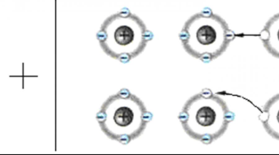
An electron-hole junction (abbreviated p-n junction) occurs in a semiconductor crystal that simultaneously has regions with n-type (contains donor impurities) and p-type (with acceptor impurities) conductivities at the boundary between these regions.
Let's say we have a crystal in which there is a semiconductor region with hole (p-type) conductivity on the left, and with electronic (n-type) conductivity on the right (Fig. 10). Thanks to thermal movement When a contact is formed, electrons from the n-type semiconductor will diffuse into the p-type region. In this case, an uncompensated positive donor ion will remain in the n-type region. Having passed into the region with hole conductivity, the electron very quickly recombines with the hole, and an uncompensated acceptor ion is formed in the p-type region.

Similar to electrons, holes from the p-type region diffuse into the electron region, leaving an uncompensated negatively charged acceptor ion in the hole region. Having passed into the electronic region, the hole recombines with an electron. As a result, an uncompensated positive donor ion is formed in the electronic region.
As a result of diffusion, a double electric layer of oppositely charged ions is formed at the boundary between these regions, the thickness l which does not exceed fractions of a micrometer.
An electric field with a strength of E i. The electric field of an electron-hole junction (pn junction) prevents electrons and holes from moving further across the interface between the two semiconductors. The blocking layer has increased resistance compared to other volumes of semiconductors.
External electric field with intensity E affects the resistance of the blocking electric field. If the n-semiconductor is connected to the negative pole of the source, and the plus of the source is connected to the p-semiconductor, then under the influence of an electric field, electrons in the n-semiconductor and holes in the p-semiconductor will move towards each other towards the interface of the semiconductors (Fig. 11). Electrons, crossing the border, “fill” holes. With such a forward direction of the external electric field, the thickness of the blocking layer and its resistance continuously decrease. In this direction, electric current passes through the pn junction.

The considered direction of the pn junction is called direct. The dependence of current on voltage, i.e. volt-ampere characteristics direct transition, shown in Fig. 12 with a solid line.

If the n-semiconductor is connected to the positive pole of the source, and the p-semiconductor to the negative, then electrons in the n-semiconductor and holes in the p-semiconductor under the influence of the electric field will move from the interface in opposite directions (Fig. 13). This leads to a thickening of the barrier layer and an increase in its resistance. The direction of the external electric field that expands the blocking layer is called locking (reverse). With this direction of the external field, the electric current of the main charge carriers does not pass through the contact of two p- and p-semiconductors.

The current through the pn junction is now due to the electrons present in the p-type semiconductor and the holes from the n-type semiconductor. But there are very few minority charge carriers, so the conductivity of the junction turns out to be insignificant, and its resistance is large. The considered direction of the pn junction is called reverse, its current-voltage characteristic is shown in Fig. 12 dashed line.
Please note that the scale of current measurement for forward and reverse transitions differs by a thousand times.
Note that at a certain voltage applied in the opposite direction, breakdown(i.e. destruction) of the p-n junction.
Semiconductor devices
Thermistors
The electrical resistance of semiconductors is highly dependent on temperature. This property is used to measure temperature by current strength in a circuit with a semiconductor. Such devices are called thermistors or thermistors. The semiconductor substance is placed in a metal protective case, in which there are insulated terminals for connecting the thermistor to the electrical circuit.
Changing the resistance of thermistors when heating or cooling allows them to be used in temperature measuring instruments to maintain a constant temperature in automatic devices- in closed thermostat chambers, to provide fire alarms, etc. There are thermistors for measuring both very high ( T≈ 1300 K) and very low ( T≈ 4 - 80 K) temperatures.
A schematic representation (Fig. a) and photograph (Fig. b) of the thermistor is shown in Figure 14.
 Rice. 14
 Photoresistors
The electrical conductivity of semiconductors increases not only when heated, but also when illuminated. Electrical conductivity increases due to the breaking of bonds and the formation of free electrons and holes due to the energy of light incident on the semiconductor.
Devices that take into account the dependence of the electrical conductivity of semiconductors on lighting are called photoresistors.
The materials for the manufacture of photoresistors are compounds such as CdS, CdSe, PbS and a number of others.
The miniature size and high sensitivity of photoresistors allow them to be used for recording and measuring weak light fluxes. Photoresistors are used to determine the quality of surfaces, control the dimensions of products, etc.
A schematic representation (Fig. a) and photograph (Fig. b) of the photoresistor is shown in Figure 15.
 Rice. 15
 Semiconductor diode
The ability of a pn junction to pass current in one direction is used in semiconductor devices called diodes.
Semiconductor diodes are made from germanium, silicon, selenium and other substances.
To prevent harmful effects air and light, the germanium crystal is placed in a hermetically sealed metal case. Semiconductor diodes are the main elements of AC rectifiers (more precisely, they serve to convert alternating current into a pulsating direct current.)
A schematic representation (Fig. a) and photograph (Fig. b) of a semiconductor diode is shown in Figure 16.
 Rice. 16
 LEDs
Light-emitting diode or light emitting diode- a semiconductor device with a p-n junction that creates optical radiation when an electric current is passed through it.
The emitted light lies in a narrow range of the spectrum, its spectral characteristics depend, among other things, on chemical composition semiconductors used in it.
Literature
- Aksenovich L. A. Physics in high school: Theory. Tasks. Tests: Textbook. allowance for institutions providing general education. environment, education / L. A. Aksenovich, N. N. Rakina, K. S. Farino; Ed. K. S. Farino. - Mn.: Adukatsiya i vyakhavanne, 2004. - P. 300-308.
- Burov L.I., Strelchenya V.M. Physics from A to Z: for students, applicants, tutors. - Mn.: Paradox, 2000. - P. 219-228.
- Myakishev G. Ya. Physics: Electrodynamics. 10 – 11 grades: textbook for in-depth study of physics / G.Ya. Myakishev, A.Z. Sinyakov, B.A. Slobodskov. - M.: Bustard, 2005. - P. 309-320.
- Yavorsky B. M., Seleznev Yu. A. A reference guide to physics for those entering universities and self-education. - M.: Nauka, 1984. - P. 165-169.
Lesson No. 41-169 Electric current in semiconductors. Semiconductor diode. Semiconductor devices.
A semiconductor is a substance in which the resistivity can vary over a wide range and decreases very quickly with increasing temperature, which means that the electrical conductivity increases. It is observed in silicon, germanium, selenium and in some compounds. Conduction mechanism in semiconductors
Semiconductor crystals have an atomic crystal lattice where outer electrons are bonded to neighboring atoms by covalent bonds. At low temperatures, pure semiconductors have no free electrons and behave like an insulator. If the semiconductor is pure (without impurities), then it has its own conductivity (small). Intrinsic conductivity is of two types: 1) electronic (conductivity " P"-type) At low temperatures in semiconductors, all electrons are associated with the nuclei and the resistance is high; As the temperature increases, the kinetic energy of the particles increases, bonds break down and free electrons appear - the resistance decreases. Free electrons move opposite to the electric field strength vector. The electronic conductivity of semiconductors is due to the presence free electrons. 2) hole ("p"-type conductivity). With increasing temperature, covalent bonds between valence electrons are destroyed and places with a missing electron are formed - a "hole". its place can be replaced by valence electrons. The movement of the “hole” is equivalent to the movement of a positive charge. The movement of the hole occurs in the direction of the electric field strength vector. The breaking of covalent bonds and the emergence of intrinsic conductivity of semiconductors can be caused by heating, illumination (photoconductivity) and the action of strong electric fields.  Dependence R(t): thermistor
- remote measurement t; - fire alarm
 1) donor impurities (giving away) - are additional suppliers of electrons to semiconductor crystals, easily donate electrons and increase the number of free electrons in the semiconductor. These are the conductors" n "-type, i.e. semiconductors with donor impurities, where the main charge carrier is electrons, and the minority charge carrier is holes. Such a semiconductor has electronic impurity conductivity (for example, arsenic). 2
 ) acceptor impurities (receivers) create “holes” by taking electrons into themselves. These are “p”-type semiconductors, i.e. semiconductors with acceptor impurities, where the main charge carrier is holes, and the minority - electrons. Such a semiconductor has hole impurity conductivity (example - indium). Electrical properties "p-
n"transitions."pn" junction (or electron-hole junction) is the area of contact of two semiconductors where the conductivity changes from electronic to hole (or vice versa). IN
) acceptor impurities (receivers) create “holes” by taking electrons into themselves. These are “p”-type semiconductors, i.e. semiconductors with acceptor impurities, where the main charge carrier is holes, and the minority - electrons. Such a semiconductor has hole impurity conductivity (example - indium). Electrical properties "p-
n"transitions."pn" junction (or electron-hole junction) is the area of contact of two semiconductors where the conductivity changes from electronic to hole (or vice versa). IN  Such regions can be created in a semiconductor crystal by introducing impurities. In the contact zone of two semiconductors with different conductivities, mutual diffusion of electrons and holes will take place and a blocking barrier will be formed. electric layer. The electric field of the barrier layer preventsfurther transition of electrons and holes across the boundary. The blocking layer has increased resistance compared to other areas of the semiconductor. IN
  The external electric field affects the resistance of the barrier layer. In the forward (through) direction of the external electric field, the current passes through the boundary of two semiconductors. Because electrons and holes move towards each other towards the interface, then the electrons crossing the border, they fill the holes. The thickness of the barrier layer and its resistance are continuously decreasing.
P  With a blocking (reverse direction of the external electric field) current will not pass through the contact area of the two semiconductors. Because electrons and holes move from the boundary in opposite directions, then the blocking layer thickens, its resistance increases. Thus, the electron-hole transition has one-way conductivity.
Semiconductor diode- semiconductor with one p-n junction.P  Semiconductor diodes are the main elements of AC rectifiers.
When an electric field is applied: in one direction the resistance of the semiconductor is high, in the opposite direction the resistance is low.
Transistors.(from English words transfer - transfer, resistor - resistance) Let's consider one of the types of transistors made of germanium or silicon with donor and acceptor impurities introduced into them. The distribution of impurities is such that a very thin (on the order of several micrometers) layer of n-type semiconductor is created between two layers of p-type semiconductor (see figure).  This thin layer is called basis or base. Two are formed in the crystal R-n junctions whose forward directions are opposite. Three outputs from areas with various types conductivity allow you to include a transistor in the circuit shown in the figure. With this switch on, the left R-n-transition is direct and separates the base from the region with p-type conductivity, called emitter. If there were no right R-n-junction, in the emitter-base circuit there would be a current depending on the voltage of the sources (batteries B1 and AC voltage source) and circuit resistance, including the low resistance of the direct emitter-base junction. Battery B2 turned on so that the right R The -n junction in the circuit (see figure) is reverse. It separates the base from the right region with p-type conductivity, called collector. If there was no left R-n junction, the current in the collector circuit would be close to zero, since the resistance of the reverse junction is very high. If there is a current in the left R-n junction, a current appears in the collector circuit, and the current in the collector is only slightly less than the current in the emitter (if a negative voltage is applied to the emitter, then the left R-n-junction will be reverse and there will be practically no current in the emitter circuit and in the collector circuit). When a voltage is created between the emitter and the base, the majority carriers of a p-type semiconductor - holes - penetrate into the base, where they are already minority carriers. Since the thickness of the base is very small and the number of majority carriers (electrons) in it is small, the holes that get into it almost do not combine (do not recombine) with the electrons of the base and penetrate into the collector due to diffusion. Right R The -n junction is closed to the main charge carriers of the base - electrons, but not to holes. In the collector, holes are carried away by the electric field and complete the circuit. The strength of the current branching into the emitter circuit from the base is very small, since the cross-sectional area of the base in the horizontal (see figure above) plane is much smaller than the cross-section in the vertical plane.
The current in the collector, which is almost equal to the current in the emitter, changes along with the current in the emitter. Resistor R has little effect on the collector current, and this resistance can be made quite large. By controlling the emitter current using an alternating voltage source connected to its circuit, we obtain a synchronous change in the voltage across the resistor R .
With a large resistance of the resistor, the change in voltage across it can be tens of thousands of times greater than the change in signal voltage in the emitter circuit. This means increased tension. Therefore, at load R it is possible to obtain electrical signals whose power is many times greater than the power entering the emitter circuit.
Application of transistors Properties R-n junctions in semiconductors are used to amplify and generate electrical oscillations.

3
Semiconductors are materials that are dielectrics under normal conditions, but become conductors with increasing temperature. That is, in semiconductors, as the temperature increases, the resistance decreases.
The structure of a semiconductor using the example of a silicon crystal
Let's consider the structure of semiconductors and the main types of conductivity in them. As an example, consider a silicon crystal.
Silicon is a tetravalent element. Consequently, in its outer shell there are four electrons that are weakly bound to the nucleus of the atom. Each one has four more atoms in its neighborhood.
Atoms interact with each other and form covalent bonds. One electron from each atom participates in such a bond. The silicon device diagram is shown in the following figure.
picture
Covalent bonds are quite strong and do not break at low temperatures. Therefore, there are no free charge carriers in silicon, and at low temperatures it is a dielectric. There are two types of conductivity in semiconductors: electron and hole.
Electronic conductivity
When silicon is heated, additional energy will be imparted to it. Kinetic energy particles increases and some covalent bonds are broken. This creates free electrons.
In an electric field, these electrons move between the nodes of the crystal lattice. In this case, an electric current will be created in the silicon.
Since the main charge carriers are free electrons, this type of conductivity is called electronic conductivity. The number of free electrons depends on temperature. The more we heat silicon, the more covalent bonds will be broken, and therefore more free electrons will appear. This leads to a decrease in resistance. And silicon becomes a conductor.
Hole conductivity
When a covalent bond breaks, a vacant place, which can be occupied by another electron. This place is called a hole. The hole has an excess positive charge.
The position of the hole in the crystal is constantly changing; any electron can occupy this position, and the hole will move to the place where the electron jumped from. If there is no electric field, then the movement of the holes is random, and therefore no current occurs.
In its presence, an orderly movement of holes arises, and in addition to the current that is created free electrons, another current appears, which is created by the holes. The holes will move in the opposite direction to the electrons.
Thus, in semiconductors, conductivity is electron-hole. Current is created by both electrons and holes. This type of conductivity is also called intrinsic conductivity, since elements of only one atom are involved.